Tag Archive for: PCB Connector

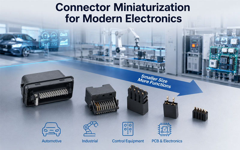
Connector Miniaturizationfor Modern Electronics

Modern electronic systems are becoming smaller, lighter, and more integrated.

Devices that once had plenty of internal space now need to accommodate more functions within increasingly compact packages.

This trend has created strong demand for smaller and higher-density connectors.

However, making a connector smaller is not simply a matter of reducing the housing dimensions.

As connector size decreases, the available space for contacts, insulation, mechanical structures, sealing, and assembly also becomes smaller.

At the same time, electrical and mechanical requirements often remain the same—or become more demanding.

Connector miniaturization therefore requires a careful balance between:

Size + Electrical Performance + Mechanical Reliability + Manufacturability

For applications such as automotive electronics, industrial automation, medical equipment, consumer electronics, robotics, and compact control systems, successful miniaturization requires engineering optimization at every stage.
Connector Miniaturizationfor Modern Electronics


What Is Connector Miniaturization?

Connector miniaturization refers to reducing the physical size, pitch, height, or overall footprint of a connector while maintaining its required functional performance.

Miniaturization may involve:

  • Smaller housing dimensions
  • Reduced contact pitch
  • Smaller terminals
  • Lower connector height
  • Higher contact density
  • Reduced mounting footprint

The goal is usually to achieve:

More electrical functionality in less physical space.

However, reducing dimensions can create new engineering constraints.


Why Are Connectors Becoming Smaller?

Several market trends are driving connector miniaturization.

Smaller Electronic Devices

Electronic products increasingly require:

  • Compact control units
  • Smaller sensors
  • Reduced PCB size
  • Higher functional density

Connectors must fit within these increasingly constrained spaces.


Higher Functional Integration

A single electronic module may now integrate:

  • Power
  • Data
  • Sensors
  • Control signals
  • Communication interfaces

This increases the number of electrical connections required within the same physical space.


Weight Reduction

In automotive and portable equipment, reducing component size can also contribute to overall weight reduction.

Smaller connectors can help optimize:

  • Wiring space
  • Module dimensions
  • Packaging
  • System weight

1.Contact Pitch Becomes More Challenging

One of the biggest challenges in connector miniaturization is reducing contact pitch.

As the distance between contacts decreases, engineers must maintain sufficient:

  • Electrical isolation
  • Mechanical strength
  • Positioning accuracy
  • Insulation performance

A smaller pitch leaves less room for dimensional variation.

This makes:

Terminal Position + Housing Accuracy + Manufacturing Tolerance

increasingly important.


2.Electrical Clearance Becomes More Limited

When contacts are positioned closer together, the available electrical spacing decreases.

Engineers need to evaluate:

  • Clearance
  • Creepage
  • Insulation thickness
  • Working voltage
  • Pollution environment

For higher-voltage applications, simply reducing contact spacing may not be possible without changing the connector architecture.

This creates a fundamental design challenge:

How can the connector become smaller without compromising electrical safety?


3.Current Density Can Increase

Miniaturization can also increase current density.

If the same current must pass through a smaller terminal, the available conductive cross-section may decrease.

This can increase:

  • Current density
  • Joule heating
  • Contact temperature
  • Thermal stress

The design must therefore balance:

Contact Size + Material Conductivity + Contact Resistance + Current Rating

A smaller connector is not automatically suitable for the same current level as a larger connector.


4.Thermal Management Becomes More Difficult

Heat generated at a connector contact must be transferred away from the contact interface.

When connector dimensions decrease:

  • Thermal paths may become smaller
  • Contact spacing may decrease
  • Heat concentration can increase
  • Cooling space may be reduced

This can become particularly important in:

  • High-current applications
  • Compact automotive modules
  • Industrial control systems
  • Power electronics

Thermal design should therefore be considered alongside electrical design.


5.Contact Spring Design Becomes More Sensitive

Smaller terminals have less physical space for spring structures.

However, the contact still needs sufficient force to maintain reliable electrical connection.

The challenge becomes:

Small Contact + Controlled Spring Force + Long-Term Reliability

If spring force is too low:

  • Contact resistance may increase
  • Vibration resistance may decrease
  • Intermittent connections may occur

If spring force is too high:

  • Mating force increases
  • Contact wear may accelerate
  • Mating cycle life may decrease

Miniaturization therefore requires highly controlled contact geometry.


6.Mechanical Strength Can Be Reduced

Reducing terminal and housing dimensions can reduce structural strength.

Miniature connectors may be more sensitive to:

  • Insertion force
  • Extraction force
  • Cable pulling
  • Side loading
  • Vibration
  • Shock

The housing must therefore maintain sufficient:

  • Retention strength
  • Locking performance
  • Terminal support
  • Mechanical stability

Miniaturization should never compromise the mechanical integrity of the connector.


7.Manufacturing Tolerances Become More Critical

As components become smaller, the same absolute dimensional variation represents a larger percentage of the total geometry.

For example, a small terminal-position variation may have little effect in a large connector but become significant in a fine-pitch connector.

Critical areas include:

  • Terminal pitch
  • Terminal position
  • Housing cavities
  • Locking features
  • Contact geometry
  • Seal interfaces

This makes precision manufacturing and tolerance control increasingly important.


8.Assembly Becomes More Difficult

Smaller connector components can be more challenging to assemble.

Potential problems include:

  • Terminal misalignment
  • Incomplete terminal insertion
  • Seal damage
  • Housing deformation
  • Locking errors

Manual assembly becomes more difficult as component size decreases.

For high-volume production, manufacturers may need:

  • Precision assembly fixtures
  • Automated insertion
  • Vision inspection
  • Automated electrical testing

9.Inspection Becomes More Challenging

Miniaturized features may be difficult to inspect using conventional measurement methods.

Traditional tools may not provide sufficient resolution or repeatability.

Manufacturers may therefore use:

  • Optical inspection
  • CCD systems
  • Microscopic inspection
  • Coordinate measurement
  • Automated dimensional analysis

Inspection strategies must be designed around the actual critical features of the connector.


10.Miniaturization Can Affect Mating Reliability

Smaller connectors may have less mechanical tolerance for misalignment.

During mating, even a small angular or positional deviation can influence:

  • Insertion force
  • Terminal engagement
  • Contact wipe
  • Housing alignment

Good guiding features become increasingly important.

Common design solutions include:

  • Polarization keys
  • Guide posts
  • Chamfered mating surfaces
  • Self-alignment structures

These features help reduce the risk of incorrect or incomplete mating.


11.Sealing Becomes More Difficult

For miniature waterproof connectors, the available space for seals is limited.

Yet the connector may still need to achieve:

  • IP67
  • IP68
  • Other application-specific sealing requirements

Engineers must optimize:

  • Seal geometry
  • Compression
  • Housing interfaces
  • Cable diameter
  • Material selection

Reducing the connector size without compromising sealing performance can be challenging.


12.Miniaturization and Mating Cycles

A smaller connector does not necessarily have a shorter mating life, but reducing contact dimensions can make wear management more difficult.

Each mating cycle may affect:

  • Contact plating
  • Spring structure
  • Contact surface
  • Housing alignment

For applications requiring frequent connection and disconnection, engineers should validate:

  • Insertion force
  • Extraction force
  • Contact resistance
  • Wear
  • Mating cycle performance

13.Material Selection Becomes More Important

Material selection can become more critical as connector dimensions decrease.

The housing material must provide appropriate:

  • Mechanical strength
  • Dimensional stability
  • Temperature resistance
  • Electrical insulation

Contact materials must provide:

  • Conductivity
  • Elasticity
  • Fatigue resistance
  • Corrosion resistance

For miniature connectors, small changes in material performance can have a noticeable impact on the overall system.


14.Miniaturization Requires Better Thermal and Electrical Simulation

For advanced connector designs, simulation can help evaluate potential problems before tooling.

Depending on the application, engineers may evaluate:

Electrical

  • Current density
  • Voltage distribution
  • Contact resistance

Thermal

  • Temperature rise
  • Heat concentration
  • Thermal paths

Mechanical

  • Contact deformation
  • Stress distribution
  • Mating force

Simulation does not replace physical testing, but it can help identify design risks earlier.


Miniaturization Trade-Offs

Connector miniaturization is fundamentally an optimization problem.

Design GoalPotential Challenge
Smaller housingLess internal space
Higher contact densityReduced spacing
Higher currentGreater heat generation
Lower mating forcePotentially lower contact force
Smaller terminalsReduced mechanical strength
Smaller sealsMore difficult sealing
Tight tolerancesHigher manufacturing cost
More featuresMore complex assembly

The objective is not simply:

Make It Smaller.

The objective is:

Make It Smaller Without Losing Performance.


Application Considerations

Different applications have different miniaturization priorities.

ApplicationKey Miniaturization Challenge
Automotive ElectronicsSpace, vibration, temperature
Medical EquipmentCompactness, reliability, cleanliness
Industrial AutomationDensity, mechanical durability
RoboticsSize, movement, mating cycles
Consumer ElectronicsSpace and high-density interconnection
SensorsCompact size and environmental protection
Control ModulesDensity, thermal management, assembly

How to Approach Miniature Connector Design

A successful miniature connector development process should include:

Step 1: Define the Application

Identify:

  • Voltage
  • Current
  • Signal type
  • Temperature
  • Vibration
  • Mating cycles
  • Environmental exposure

Step 2: Establish the Size Target

Define:

  • Maximum housing dimensions
  • Contact pitch
  • Mounting footprint
  • Connector height

Step 3: Design the Contact System

Optimize:

  • Contact geometry
  • Spring force
  • Contact material
  • Plating
  • Current capacity

Step 4: Analyze Thermal and Electrical Performance

Evaluate:

  • Contact resistance
  • Temperature rise
  • Current density
  • Clearance
  • Creepage

Step 5: Perform Tolerance Analysis

Review:

  • Terminal position
  • Housing dimensions
  • Mating alignment
  • Locking features
  • Seal interfaces

Step 6: Validate Through Testing

Typical validation can include:

  • Contact resistance
  • Temperature rise
  • Insertion/extraction force
  • Mating cycles
  • Vibration
  • Thermal cycling
  • Environmental testing

Common Connector Miniaturization Mistakes

MistakePotential Result
Reducing size without thermal analysisExcessive temperature rise
Reducing contact pitch excessivelyElectrical clearance problems
Undersized terminalHigher current density
Insufficient spring forceUnstable contact
Excessive spring forceHigh mating force
Ignoring tolerance stack-upMating problems
Weak housing structureMechanical failure
Poor seal designWater or dust ingress
Insufficient inspectionManufacturing variation

How FPIC Supports Connector Miniaturization

FPIC supports customized connector development with engineering capabilities covering:

✔ Contact system design

✔ Housing design

✔ Terminal stamping

✔ Precision injection molding

✔ Tolerance control

✔ Electrical testing

✔ Mechanical reliability testing

✔ CCD/visual inspection

✔ Automated assembly and packaging

For demanding automotive applications, FPIC’s connector manufacturing capabilities are supported by IATF 16949 quality management requirements.

Connector production can also incorporate controlled cleanliness practices aligned with VDA 19.1 / ISO 16232 requirements where applicable.

The engineering objective is to optimize connector size without sacrificing:

  • Electrical performance
  • Mechanical reliability
  • Manufacturing consistency
  • Service life

Final Thoughts

Connector miniaturization is one of the most important trends in modern electronics.

But reducing connector dimensions creates a chain of engineering challenges.

Smaller connectors require careful control of:

Contact Density + Electrical Clearance + Thermal Performance + Spring Force + Mechanical Strength + Manufacturing Tolerance

The best miniature connector is not simply the smallest possible connector.

It is the smallest connector that can reliably meet its electrical, mechanical, environmental, manufacturing, and lifecycle requirements.

Successful miniaturization therefore requires a system-level approach:

Define → Design → Simulate → Manufacture → Test → Validate

When size reduction is combined with disciplined engineering and manufacturing control, miniature connectors can deliver high-density performance without compromising reliability.


FAQ

What is connector miniaturization?

Connector miniaturization is the process of reducing connector size, contact pitch, height, or mounting footprint while maintaining required electrical and mechanical performance.

What is the biggest challenge in miniature connector design?

There is no single challenge. Contact density, electrical clearance, thermal management, mechanical strength, manufacturing tolerance, and assembly precision often become more difficult simultaneously.

Does a smaller connector support less current?

Not necessarily, but reducing terminal size and conductive area can increase current density and heat generation. Current capability must be evaluated based on the complete contact design and application conditions.

Why are manufacturing tolerances important for miniature connectors?

As connector features become smaller, the same dimensional variation can have a greater functional impact, especially on terminal alignment, mating, and contact performance.

How can miniature connectors maintain reliability?

Reliable miniature connectors require optimized contact geometry, suitable materials and plating, controlled tolerances, appropriate thermal design, precise manufacturing, and application-specific validation.


Need a Compact Connector for a Space-Constrained Application?

FPIC supports custom connector development from contact design and tooling through precision manufacturing, testing, and mass production.

Whether you need compact signal connectors, circular connectors, automotive connectors, or customized high-density solutions, our engineering team can help balance size, performance, reliability, and manufacturability.

Contact FPIC to discuss your miniature connector requirements.


Resources

  1. IEC 60512 – Connectors for Electronic Equipment – Tests and Measurements
    https://www.iec.ch/
    International testing framework for electrical and mechanical performance of connectors.
  2. USCAR Standards
    https://www.uscar.org/
    Automotive connector performance and validation resources.
  3. IPC Standards
    https://www.ipc.org/
    Industry standards and technical resources for electronic interconnection and manufacturing.
  4. IATF 16949
    https://www.iatfglobaloversight.org/
    Automotive quality management requirements for organizations in the automotive supply chain.
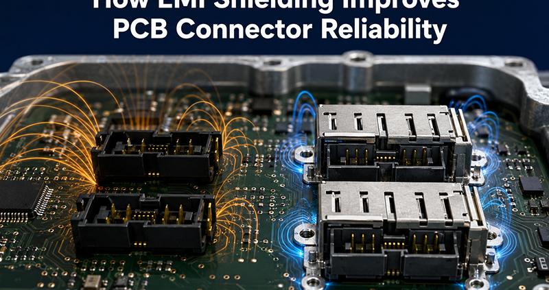
Smaller electronic systems increasingly combine high-speed signals, wireless functions, power conversion, sensors, and control circuits on densely populated PCBs. Under these conditions, connector selection affects more than pin count and mating height.

A compact connector must also support signal integrity, current delivery, mechanical stability, manufacturability, and electromagnetic compatibility.

Quick Answer:

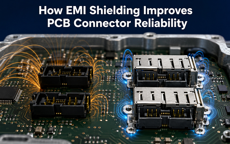
EMI shielding improves PCB connector reliability by limiting electromagnetic energy entering or leaving the connection interface. An effective shield, combined with a low-impedance grounding path and correct PCB layout, can reduce noise, crosstalk, data errors, and EMC compliance risks.

Molex’s recent Quad-Row Shield announcement illustrates this industry direction. The connector combines a four-row contact layout with an integrated metal shield. Molex reports up to a 25 dB EMI reduction compared with its unshielded Quad-Row version, while samples are available for custom inquiries and commercial supply is planned for the second quarter of 2026.

However, a metal cover alone does not guarantee reliable electromagnetic performance. Engineers must evaluate the connector, PCB grounding, enclosure, contact layout, cable paths, power distribution, and application environment as one system.


Why EMI Becomes More Difficult in Compact PCB Systems

Miniaturization places more electrical functions into a smaller physical area. Signal traces, power contacts, antennas, switching regulators, clocks, processors, sensors, and communication circuits may operate only millimeters apart.

This creates several potential interference paths:

  • noise generated by switching power circuits;
  • radiation from high-speed digital signals;
  • coupling between adjacent contacts;
  • interference entering through openings in an enclosure;
  • current flowing through poorly controlled ground paths;
  • transient noise from motors, relays, converters, or wireless transmitters.

A conventional connector may provide adequate electrical continuity while still allowing interference to couple across the board interface.

This is particularly important when the system includes:

  • high-speed serial communication;
  • cameras or display modules;
  • radar or wireless functions;
  • compact automotive control modules;
  • medical or measuring equipment;
  • industrial sensors and controllers;
  • mixed power-and-signal interfaces.

Molex identifies controlled impedance, reduced crosstalk, and EMI shielding as important features for optimizing PCB layout, signal integrity, and system performance in mezzanine connectors.

What EMI Shielding Does at the Connector Interface

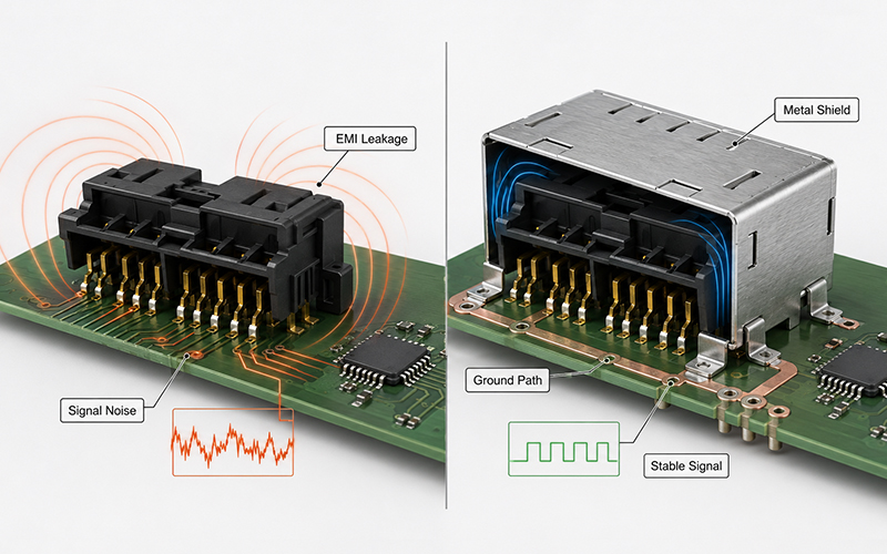
A connector shield forms a conductive barrier around or near the signal contacts. When properly grounded, this structure helps control electromagnetic fields around the mating interface.

Its primary functions include:

What EMI Shielding Does at the Connector Interface

1. Reducing Radiated Emissions

Fast signal edges and switching currents can cause the connector and adjacent PCB structures to radiate electromagnetic energy.

A conductive shield helps contain part of this energy before it reaches nearby circuits, antennas, sensors, or the external environment.

2. Improving Immunity to External Noise

The same barrier can reduce the amount of external interference that reaches sensitive contacts.

This becomes important when connectors operate near:

  • DC/DC converters;
  • motors and actuators;
  • wireless antennas;
  • high-current conductors;
  • relays and solenoids;
  • vehicle power electronics.

3. Controlling Crosstalk

Crosstalk occurs when energy from one signal path couples into another.

Shielding can reduce field coupling, but pin assignment, contact spacing, ground-contact placement, differential-pair routing, and return-path design remain equally important.

4. Supporting EMC Compliance

Integrated shielding may simplify the path toward electromagnetic compatibility because it controls interference closer to the source.

Molex states that its shielded Quad-Row design can reduce EMI, support stringent EMI/EMC requirements, and lower the regulatory testing burden. This is a supplier-reported product benefit rather than a guarantee that any completed device will pass certification automatically.

The complete product must still be tested in its final configuration.


Shielding Effectiveness Depends on the Ground Path

One of the most common design errors is treating the metal shield as an isolated component.

A shield only works effectively when interference current can flow through a controlled, low-impedance path to ground or chassis.

Engineers should examine:

  • how the shield contacts the PCB;
  • the number and location of grounding points;
  • the length of the grounding path;
  • PCB ground-plane continuity;
  • enclosure contact around the interface;
  • gaps between mating shield components;
  • whether the shield remains continuous after mating.

At higher frequencies, a long or narrow grounding path can behave inductively. This limits the shield’s effectiveness even when DC continuity appears satisfactory.

For this reason, shielding design should begin during connector and PCB development—not after the first EMC test failure.

How EMI Shielding Improves PCB Connector Reliability

EMI Shielding and Signal Integrity Are Related but Different

EMI and signal integrity are closely connected, but they are not identical.

EMI design controls unwanted electromagnetic energy entering or leaving a system.

Signal-integrity design ensures that the intended signal reaches the receiver with acceptable timing, amplitude, noise margin, and waveform quality.

A shield may reduce external noise while the signal still suffers from:

  • impedance discontinuity;
  • reflections;
  • poor return paths;
  • excessive insertion loss;
  • skew between differential traces;
  • crosstalk inside the contact field.

For high-speed interfaces, engineers may need to evaluate:

  • insertion loss;
  • return loss;
  • near-end and far-end crosstalk;
  • differential impedance;
  • S-parameters;
  • eye-diagram performance;
  • contact assignment and grounding strategy.

Molex states that preferred pin layouts and S-parameter input specifications may be assigned within the 80-pin Quad-Row Shield design. This shows that shielding and contact mapping must be engineered together rather than evaluated separately.


Miniaturization Must Not Reduce Power Reliability

Modern compact connectors increasingly carry both signal and power.

This creates a difficult design balance:

  • more contacts in less PCB area;
  • higher current density;
  • less space for heat dissipation;
  • greater sensitivity to contact resistance;
  • stronger interaction between power noise and signal circuits.

Molex describes its Quad-Row architecture as supporting up to 80 pins and substantially more signal and power connections than a single-pin interface. Its product page lists current capability in the approximate 2.6–3.0 A-per-contact range for typical configurations, while the wider Molex board-to-board portfolio includes different product families for substantially higher current requirements.

This does not mean every contact can carry the maximum value simultaneously under all conditions.

Current capability depends on:

  • conductor and terminal geometry;
  • number of simultaneously energized contacts;
  • contact resistance;
  • ambient temperature;
  • PCB copper area;
  • enclosure airflow;
  • duty cycle;
  • permitted temperature rise.

When power and sensitive signals share one interface, engineers should consider using dedicated ground contacts, separating power from high-speed pairs, and validating the final assembly through temperature-rise and electrical testing.


When Does a PCB Connector Need EMI Shielding?

Not every application requires a shielded interface.

Adding shielding can increase component complexity, tooling requirements, PCB grounding needs, and cost. It should therefore solve a defined electromagnetic problem.

Shielding deserves serious consideration when one or more of the following conditions apply.

1. High-Speed Signals Cross the Interface

Interfaces carrying high-speed differential data, camera signals, displays, radar data, Ethernet, or other fast digital communication are more sensitive to discontinuities and interference.

2. The Connector Is Close to a Noise Source

Risk increases when the connector sits near switching regulators, high-current traces, motors, relays, inverters, wireless transmitters, or inductive loads.

3. The Product Has Limited Enclosure Shielding

A plastic enclosure or a large opening around the connector may offer little control over radiated energy.

An integrated connector shield can help close part of this electromagnetic gap.

4. The System Has Strict EMC Requirements

Automotive, industrial, medical, aerospace, and communication equipment often face demanding immunity and emission requirements.

A shielded interface may provide additional design margin, although system-level testing remains necessary.

5. Power and Signal Contacts Share Limited Space

Mixed power-and-signal layouts may introduce switching noise, ground bounce, and thermal constraints.

Shielding can be part of the solution, but contact allocation and PCB return-path design are equally important.


Connector Shielding Cannot Correct a Poor PCB Layout

A shielded component may still perform poorly when the surrounding PCB layout creates uncontrolled interference paths.

Engineers should coordinate the connector design with the board layout.

1. Maintain a Continuous Reference Plane

High-speed signals need a stable return path.

Avoid unnecessary ground-plane splits beneath the connector and around the signal escape region.

2. Place Ground Connections Close to the Shield

Short, wide ground connections generally provide lower impedance than long, narrow traces.

Multiple grounding points may improve current distribution and reduce shield discontinuities.

3. Separate Sensitive Signals from Noisy Power Paths

Avoid routing sensitive differential pairs next to switching nodes, inductors, motor outputs, or high-current conductors.

4. Minimize Stubs and Abrupt Geometry Changes

Unused branches, long breakout paths, and sudden changes in trace width or reference plane can increase reflection and noise.

5. Coordinate PCB and Enclosure Grounding

The connector shield, board ground, chassis, and external enclosure should follow a deliberate grounding strategy.

Connecting them without understanding the return-current path can create new coupling problems.

Mechanical Design Also Affects Shielding Reliability

Connector shielding must remain effective after assembly, vibration, temperature cycling, and repeated mating.

A mechanically weak shield may lose contact pressure, deform, or create gaps that reduce electromagnetic performance.

Important mechanical considerations include:

  • shield retention in the housing;
  • mating alignment;
  • solder-joint strength;
  • board hold-down features;
  • resistance to connector peeling or lifting;
  • vibration and shock resistance;
  • durability over the required mating cycles;
  • protection against handling damage.

Molex uses an armored, insert-molded nail and internal cover in its Quad-Row family to improve mechanical robustness and reduce mating damage. The company also states that the design supports conventional SMT production and high-volume reel packaging.

For automotive and industrial applications, the connector design may also need to consider:

  • temperature cycling;
  • vibration;
  • contamination;
  • housing retention;
  • pin position and coplanarity;
  • solder-joint fatigue;
  • long-term contact-force stability.

Materials and Plating Influence Electrical Performance

Shield performance depends partly on material conductivity, surface condition, mechanical force, and corrosion resistance.

The signal contacts and shield may use different base materials and plating systems according to their functions.

Typical engineering considerations include:

  • electrical conductivity;
  • spring force;
  • formability;
  • wear resistance;
  • solderability;
  • corrosion protection;
  • contact resistance;
  • compatibility with SMT temperatures.

FPIC’s technical materials identify connector contacts and shield-related parts made from copper alloys, stainless steel, and other stamped materials, with plating selected according to conductivity, solderability, corrosion resistance, and cost. They also describe high-temperature polymers such as LCP, PA9T, PA6T, PA46, and PPS for connector applications that must tolerate reflow processing.

Material selection should therefore reflect the complete production and operating environment, not only the connector’s nominal electrical rating.

How Shielded PCB Connectors Should Be Validated

A shielded connector requires more than a dimensional inspection.

Validation should combine electromagnetic, electrical, mechanical, environmental, and manufacturing checks.

Electromagnetic Evaluation

Depending on the project, testing may include:

  • shielding-effectiveness comparison;
  • radiated emissions;
  • conducted emissions;
  • radiated immunity;
  • bulk-current injection;
  • electrostatic discharge;
  • S-parameter characterization;
  • crosstalk and signal-integrity testing.

Electrical Evaluation

Common checks include:

  • contact resistance;
  • insulation resistance;
  • dielectric withstand voltage;
  • current-carrying capacity;
  • voltage drop;
  • temperature rise.

Mechanical Evaluation

Relevant tests may include:

  • mating and unmating force;
  • terminal retention;
  • connector hold-down strength;
  • vibration;
  • mechanical shock;
  • mating durability.

Environmental Evaluation

Depending on the application:

  • thermal cycling;
  • high- and low-temperature exposure;
  • humidity;
  • salt spray;
  • solder-heat resistance;
  • contamination or cleanliness inspection.

Manufacturing Evaluation

For SMT board connectors, engineers should also monitor:

  • pin coplanarity;
  • terminal position;
  • solder-joint geometry;
  • reflow compatibility;
  • pick-and-place handling;
  • shield deformation;
  • automated optical or CCD inspection.

FPIC’s internal capability materials list contact-impedance testing, temperature-rise testing, withstand-voltage and insulation testing, insertion and extraction testing, vibration, thermal shock, X-ray inspection, Keyence dimensional measurement, solder-heat evaluation, and CCD-supported automated production.

These capabilities help support design verification, but the final validation plan should always follow the customer’s application, product specification, and applicable standards.


A Practical Selection Checklist

Before choosing or developing a shielded PCB connector, define the following requirements.

Design areaInformation to confirm
Interface typeBoard-to-board, wire-to-board, header, mezzanine, or hybrid
Contact layoutPin count, pitch, row arrangement, and pin assignment
Signal requirementsProtocol, data rate, impedance, and differential pairs
Power requirementsVoltage, current per circuit, and active-contact count
Shielding objectiveEmissions, immunity, crosstalk, or enclosure continuity
GroundingPCB ground points, chassis path, and shield termination
Mechanical layoutMating height, orientation, retention, and alignment
EnvironmentTemperature, vibration, humidity, dust, and corrosion
ProductionSMT process, reflow profile, packaging, and inspection
ValidationSI, EMC, electrical, mechanical, and environmental tests

A complete requirement set prevents a project from being reduced to “same pitch, same pin count.”

Two connectors with similar dimensions may perform very differently when shielding continuity, current density, material selection, solder-joint strength, and high-speed layout are considered.


How FPIC Supports Custom PCB Connector Development

FPIC develops board-to-board, wire-to-board, automotive PCB header, receptacle, terminal, shielding, and custom interconnection components.

For compact PCB connector projects, engineering support can include:

  • application and drawing review;
  • pitch, pin-count, and mating-height evaluation;
  • contact and housing design;
  • shielding-cover and stamped-metal development;
  • signal and power contact allocation;
  • material and plating selection;
  • precision stamping and insert molding;
  • injection-mold and stamping-tool development;
  • SMT and reflow compatibility review;
  • dimensional, electrical, and mechanical verification;
  • automated assembly and CCD inspection;
  • prototype and scalable production support.

FPIC’s internal connector materials describe board-to-board products ranging from conventional pin headers to fine-pitch, high-density interfaces. They also identify applications combining high-speed signals, lower-speed circuits, and power distribution within one interface.

For automotive projects, FPIC operates under IATF 16949 and supports automotive PCB and low-voltage connector development for applications such as lighting control, power seats, window systems, multimedia modules, and related electronic control assemblies. Its broader manufacturing platform includes in-house tooling, stamping, injection molding, insert molding, automated assembly, testing, and precision-component production.

FPIC does not position every custom PCB connector as an off-the-shelf shielded high-speed product. Instead, shielding, signal performance, current capability, dimensions, materials, and validation requirements should be defined during project review.


Frequently Asked Questions

Does every board-to-board connector need EMI shielding?

No. Shielding is most valuable when high-speed signals, sensitive electronics, strong nearby noise sources, limited enclosure shielding, or strict EMC requirements create a measurable interference risk.

Can a metal connector cover guarantee EMC compliance?

No. It may improve electromagnetic performance, but final compliance depends on PCB layout, grounding, enclosure design, cables, software operating modes, power circuits, and the complete assembled product.

Does shielding improve signal integrity?

It can reduce external interference and coupling, but it cannot correct impedance discontinuities, poor differential routing, excessive loss, or an interrupted return path.

Can power and signal contacts share the same connector?

Yes, provided the contact layout, current density, temperature rise, grounding, isolation, and signal-integrity requirements are properly engineered and validated.

What information is needed for a custom shielded connector?

Provide the 2D or 3D drawings, PCB layout constraints, pitch, pin count, mating height, signal protocol, current requirements, shielding target, grounding concept, production volume, and required tests.


Conclusion

EMI shielding is becoming a functional part of compact connector design rather than an optional metal accessory.

A reliable shielded interface must combine electromagnetic control with suitable grounding, signal mapping, current capacity, thermal performance, mechanical retention, materials, SMT compatibility, and system-level validation.

For equipment manufacturers, the best connector is not simply the smallest one. It is the interface that uses limited PCB space without compromising signal quality, power delivery, production consistency, or long-term reliability.

Discuss Your Custom PCB Connector Project

FPIC supports customized automotive PCB headers, board-to-board connectors, terminals, shielding components, and complete interconnection development.

Send your drawings, PCB constraints, electrical requirements, application conditions, and forecast demand for engineering review.

Email: info@fpiconn.com


Resources

  • Molex. Molex Announces Availability of Industry-First Space-Saving Quad-Row Board-to-Board Connectors with EMI Shields. November 4, 2025.
  • Molex. Quad-Row Connectors—Features, Specifications and Applications.
  • Molex. Mezzanine Connectors.
  • Molex. Board-to-Board Connectors.